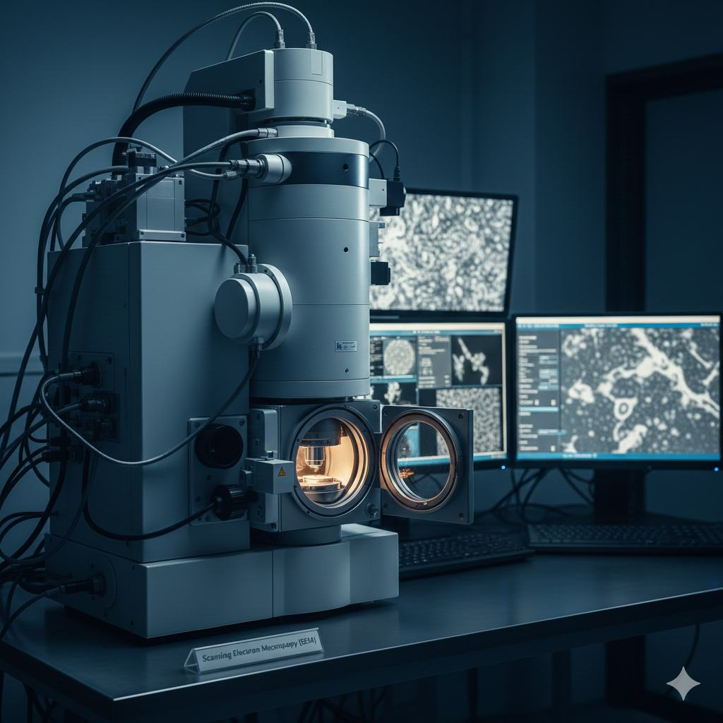
SEM EDS - Scanning Electron Microscopy with EDS
Scanning Electron Microscopy (SEM) with Energy Dispersive X-ray Spectroscopy (EDX/EDS) provides detailed imaging of surface morphology and microstructural features, along with elemental composition analysis. This powerful combination enables particle characterization, material identification, contamination assessment, failure investigations, and elemental mapping for comprehensive material evaluation.
At Diyalab, samples are assessed for compatibility, prepared as needed, and analyzed under optimized conditions to produce high-resolution, reproducible images suitable for technical evaluation and reporting.